|
by T. Mueller and R. Dumke
 n recent years we have witnessed a dramatic progress in the technological development of modern atomic physics. Prime examples of this are the invention of laser-cooling and trapping of atomic matter (Nobel Prize 1997) and the generation of quantum-degenerate gases like Bose-Einstein-Condensation (BEC) (Nobel Prize 2001). Nowadays, quantum-degenerate gases are routinely generated in physics laboratories. With the achievements in optical precision spectroscopy (see also Nobel Prize 2005) tools are available to coherently control the external and internal degrees of freedom of atomic matter. This enormous progress has led to the application of ultra cold matter in fields such as precision measurements, matter wave interferometry and applications in quantum information processing. The further development of these technologies will allow a deeper understanding in quantum physics and expanding application areas in research and technology. Controlled interactions between quantum states implemented in different physical systems are of great interest in the future development of this field. n recent years we have witnessed a dramatic progress in the technological development of modern atomic physics. Prime examples of this are the invention of laser-cooling and trapping of atomic matter (Nobel Prize 1997) and the generation of quantum-degenerate gases like Bose-Einstein-Condensation (BEC) (Nobel Prize 2001). Nowadays, quantum-degenerate gases are routinely generated in physics laboratories. With the achievements in optical precision spectroscopy (see also Nobel Prize 2005) tools are available to coherently control the external and internal degrees of freedom of atomic matter. This enormous progress has led to the application of ultra cold matter in fields such as precision measurements, matter wave interferometry and applications in quantum information processing. The further development of these technologies will allow a deeper understanding in quantum physics and expanding application areas in research and technology. Controlled interactions between quantum states implemented in different physical systems are of great interest in the future development of this field.
At our research laboratories at Nanyang Technological University (NTU) located in the School of Physical and Mathematical Sciences (SPMS) we are currently investigating novel ideas in the fields of coupled quantum systems including atomic matter, quantum information processing and precision measurements. Our projects include:
- Quantum registers for neutral atoms.
- Interaction of superconducting microstructures with atomic quantum states.
- Guided and free-space matter-wave interferometry.
To place our state-of-the-art work within the international quantum physics research community, we describe our individual projects in more detail in the following three segments.
Quantum registers for neutral atoms
Trapped ultra-cold neutral atoms are a natural candidate for qubits (quantum bits) used for quantum information processing, based on the simple quantum-level structure of atoms and good isolation from the environment [1,2]. Furthermore, with current techniques it is possible to trap and manipulate a very large ensemble of identical atoms. The systems based on neutral atoms are built on years of expertise in coherent spectroscopy, developed for application in precision measurements such as atomic clocks. In one perspective a quantum computer is nothing more than an ensemble of atomic clocks with controlled interactions between the constituent atoms. Trapped atoms can be prepared in the motional ground state of the confining trapping potential and the internal atomic states can be prepared in a desired initial state using standard of laser spectroscopy techniques. Internal-state qubits can be formed from the ground hyperfine states, which are well characterized by atomic spectroscopy and atomic-clock technology. The trapping geometry and additional fields make available a variety of choices for coherent control of the motional and internal states. Proposals for two-qubit gates rely on moving pairs of atoms into close distance to increase their coupling, or briefly turning on much stronger electric dipole interactions. To realize a system suitable for quantum information processing based on neutral atoms, the experimental design must take into account the logical encoding for qubits, the method for performing logical operations and the read-out strategy, contingent on the specific atom and trapping technology.
The design of such a system for quantum information processing with neutral atoms will depend strongly on the trapping techniques and the method for coupling atoms to each other. There are two major approaches in trapping neutral atoms: the interaction of an optical field with the atomic induced electric dipole moment or the interaction of a magnetic field with the atomic magnetic dipole moment. The most studied optical trapping method is the optical lattice [3]. An optical crystal structure is formed by the interference of intersecting laser beams. Within this light pattern electric dipole-force potential wells are generated. This virtual crystal can be dynamically controlled through the phase, polarization, wavelength and angle of the trapping laser beams. Parallel operations are natural for these highly periodic structures. Optical lattices can be loaded with many atoms from a laser-cooled ensemble or from a BEC [4]. Essential for a quantum state register is the ability to have single atom control. Loading of one atom per well in a three-dimensional lattice has been achieved using the transition to a Mott insulator [5]. A notable feature for scalability is that the character and properties of the lattice and the trapped atoms do not change in any essential way when going from a smaller to a larger lattice. Apart from these advantages, the main problem in this system is that atoms in a filled optical lattice are spaced less than a trap-laser wavelength apart, and therefore there are difficult questions about how to address individual atoms. One solution to overcome this problem is to design special trapping geometries. This has been accomplished by using engineered micro-optical devices [6-8]. It has been shown, that such devices are in principal suitable for quantum information processing purposes [9,10]. The major advantage over optical lattice structures is that the optical traps are separated far enough to easily address individual trap sites respectively and initiate, manipulate, and read out atoms in this geometry. To induce interaction between atoms at different trap sites, (essential for the realization of two qubit gates) a technique has been developed to move the traps close to each other. The major difficulty for this system is that it is not easy to trap a single atom into each trap site. Furthermore with this technique the atoms can be automatically prepared in the ground state of the lattice trapping potential.
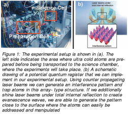 The system for quantum information processing currently being developed at NTU is a direct outgrowth of the work that has been done in optical lattices and micro optical systems. The setup and schematics are shown in Figure 1. It takes the inherent advantages of the optical lattice system and combines it with the flexibility of optical chip traps. The key idea is to use state-of-the-art devices from the quicker developing field of nano/micro optics and combine them with laser cooling and trapping technology to reach unprecedented levels of coherence and control over atomic systems. The system for quantum information processing currently being developed at NTU is a direct outgrowth of the work that has been done in optical lattices and micro optical systems. The setup and schematics are shown in Figure 1. It takes the inherent advantages of the optical lattice system and combines it with the flexibility of optical chip traps. The key idea is to use state-of-the-art devices from the quicker developing field of nano/micro optics and combine them with laser cooling and trapping technology to reach unprecedented levels of coherence and control over atomic systems.
Figure 1 shows the completed first stage of the experimental setup where we are able to prepare a ensemble of ultra-cold atoms. The sample of atoms will be later loaded into a trapping structure suitable for quantum information processing with neutral atoms.
Superconducting Atom-Chips
Superconductor technology combined with atom optical systems will allow a new generation of fundamental experiments and novel applications possibly resulting in the pairing of quantum solid-state devices with neutral atoms. In particular, the enormous capability of superconducting devices paired with atom optics is especially promising utilizing micro-structured surface traps. These can be used for quantum state transfer between solid-state and atomic systems or quantum information processing. Micro-structured surface trapping and manipulation devices, so-called 'atom chips', have proven their great capability and flexibility in the field of ultra-cold atom experiments over the last few years. These elements allow the generation of steep trapping potentials using current carrying wires or permanent magnetic structures, as well as micro-optical devices. They have been used for guiding and transportation potentials of various kinds as well as for generating quantum-degenerate gases. Additionally, the manipulation of neutral atoms with micro-structured elements is promising for realizing systems suitable for quantum information processing.
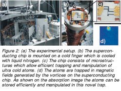 At NTU, we have began a unique project investigating the controlled interaction of superconducting quantum states with atomic quantum matter trapped on a superconducting atom chip. This innovative chip uses a high temperature superconductor for trapping and manipulating of the atomic states, which allows for a simplified experimental setup with standard laser-cooling and trapping techniques. In this project, our experiments typically produce samples of a few million atoms at temperatures of a about 0.000010 above absolute zero temperature. Once the cold sample is prepared, our experiments rely mainly on the interaction of well controlled magnetic fields with the quantized magnetic moment present in the atomic states. To reach the highest precision we employ magnetic fields created in microstructures on the chip. The structures on the chip are produced using well established technologies such as photolithography or laser ablation. This allows transferring the high precision developed for semiconductor industry to our experiments. In Figure 2, we show the typical experimental setup and an image of the chip used in our experiments. At NTU, we have began a unique project investigating the controlled interaction of superconducting quantum states with atomic quantum matter trapped on a superconducting atom chip. This innovative chip uses a high temperature superconductor for trapping and manipulating of the atomic states, which allows for a simplified experimental setup with standard laser-cooling and trapping techniques. In this project, our experiments typically produce samples of a few million atoms at temperatures of a about 0.000010 above absolute zero temperature. Once the cold sample is prepared, our experiments rely mainly on the interaction of well controlled magnetic fields with the quantized magnetic moment present in the atomic states. To reach the highest precision we employ magnetic fields created in microstructures on the chip. The structures on the chip are produced using well established technologies such as photolithography or laser ablation. This allows transferring the high precision developed for semiconductor industry to our experiments. In Figure 2, we show the typical experimental setup and an image of the chip used in our experiments.
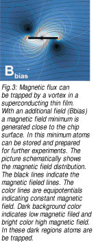
By using a high temperature superconductor a completely new field has been opened. . As a first step, we have realized a new type of magnetic interaction created by the superconducting chip. This interaction explicitly relies on quantized magnetic fields, which are present only in a superconductor. For a proof of principle experiment we have used this interaction to realize a magnetic trap for the atoms, that could significantly improve upon conventional traps based on normal conductors, since intrinsic noise sources resulting from finite electric conductivity are strongly suppressed. In the future our project will focus on exploiting the possibilities offered by this innovative type of interaction. A promising avenue is the coupling of the atomic magnetic dipole moment to the magnetic field induced by vortices inside type-II superconductors. We work towards coupling atoms to quantum states present in the superconductor in a controlled manner or even coherently. This will allow us to exploit the advantages present in each physical system, solid state and atomic matter can contribute with their different strengths to the progress towards quantum computation.
Guided and free-space matter-wave interferometer
 Today, the most precise measurements in a variety of applied sciences and engineering are performed using laser light interferometers. Examples are micro-positioning and distance measurements or the measurement of inertial forces such as accelerations or rotations. Laser gyroscopes make use of the well-developed technologies of lasers and precision optical elements. However, in comparison to optical interferometers, atom interferometers have the potential to achieve sensitivities several orders of magnitude higher for some applications. They may also enable interferometric measurements not possible with optical interferometry. An impressive list of high-precision atom-interferometric measurements of fundamental constants, atomic properties, inertial forces, and rotations has been performed [11-15]. The further development of atom interferometers and the investigation of their full potential for precision measurement and applied sensors is of high interest. Today, the most precise measurements in a variety of applied sciences and engineering are performed using laser light interferometers. Examples are micro-positioning and distance measurements or the measurement of inertial forces such as accelerations or rotations. Laser gyroscopes make use of the well-developed technologies of lasers and precision optical elements. However, in comparison to optical interferometers, atom interferometers have the potential to achieve sensitivities several orders of magnitude higher for some applications. They may also enable interferometric measurements not possible with optical interferometry. An impressive list of high-precision atom-interferometric measurements of fundamental constants, atomic properties, inertial forces, and rotations has been performed [11-15]. The further development of atom interferometers and the investigation of their full potential for precision measurement and applied sensors is of high interest.
The basic principle of atom interferometers is very similar to optical interferometers. The difference is that the optical wave is replaced with the matter-wave represented by the atoms. While the first interferometry experiments using matter waves in the 1930s is considered a prominent demonstration of quantum mechanical principles, recent progress in atomic, laser and optical technology has allowed even more impressive achievements using matter-wave interferometry. In particular the preparation of ultra-cold atoms and the achievable control of optical frequencies have led to the success of modern atom interferometry. At NTU we follow two approaches to atom interferometry for precision measurements. While one future path focuses on the advancement of currently used free-space atom interferometers, our present approach tends to the realization of guided interferometers. In this approach, the atoms are directed along one or two spatial dimensions using optical or magnetic fields, while they can freely propagate along the remaining dimension. This allows a significant enhancement of sensitivity compared to free-space approaches because the area of the interferometer can be in principal greatly extended. Our approach for a guided matter-wave interferometer makes use of specially-designed superconducting elements on a chip [16]. With our atom-interferometer chip structure, which uses a persistent current loop, it should be possible to overcome the limitations of normal conductors.
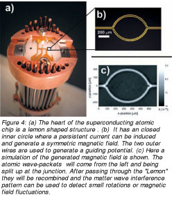 Figure 4 shows a structure similar to an optical Mach-Zehnder interferometer. The investigation of interferometry realized with matter waves propagating in the two arms of our guide is one aspect of our current project. We hope to advance the guided atom interferometer to the point where it will be a sensitive probe of inertial forces, which has several applications, e.g. in navigation. Figure 4 shows a structure similar to an optical Mach-Zehnder interferometer. The investigation of interferometry realized with matter waves propagating in the two arms of our guide is one aspect of our current project. We hope to advance the guided atom interferometer to the point where it will be a sensitive probe of inertial forces, which has several applications, e.g. in navigation.
In the future we also plan to investigate possible improvements for free-space atom interferometers, which as of now are the most precise measurement devices for a variety of quantities, e.g. physical constants or gravity. With further improvements these interferometers should allow access to new physics. Fascinating examples are the search for non-Newtonian forces on small scales or a test of the equivalence principle. By exploiting novel types of atom-optical elements and utilizing ultra-cold atomic waves with the lowest temperatures possible, we hope to make significant contributions to atom interferometry.
Outlook
Rapid progress is being made in the field of coherent manipulation of atoms in micro-traps. By combining matter wave interferometry, advanced nano-positioning of atoms using microscopic conveyors, the scalability and high flexibility in possible trapping potentials and interaction mechanisms, as well as the progress in miniaturizing experimental systems [9], the vision of portable sensors based on integrated devices may become reality in the near future. These neutral atom systems are promising candidates for the realization of quantum processors. We expect remarkable progress in the near future in this new interdisciplinary field of quantum technology.
 Click here to download the full issue for USD 6.50 Click here to download the full issue for USD 6.50
|